A team of researchers at Georgia Tech and Tianjin University has created the world’s first functional semiconductor made from graphene, a single sheet of carbon atoms held together by the strongest bonds known. Semiconductors are materials that conduct electricity under specific conditions and are foundational components of electronic devices.
Led by Walter de Heer, professor of physics at Georgia Tech, the research throws open the door to a new way of doing electronics. The breakthrough technology could allow for smaller and faster electronic devices and may have applications for quantum computing.
In a research, published on 3 January in Nature, focuses on leveraging epitaxial graphene, a crystal structure of carbon chemically bonded to silicon carbide (SiC). This novel semiconducting material, dubbed semiconducting epitaxial graphene (SEC) or — Epigraphene, which is graphene that spontaneously forms on silicon carbide crystals when silicon sublimates from the surface at high temperatures resulting in a carbon-rich surface that recrystallizes into graphene.
De Heer describes the method used as a modified version of an extremely simple technique that has been known for over 50 years. “When silicon carbide is heated to well over 1,000 °C, silicon evaporates from the surface, leaving a carbon-rich surface which then forms into graphene,” says de Heer.
Graphene, in a natural form, is neither a semiconductor nor a metal, but a sem-imetal. A band gap is a material that can be turned on and off when an electric field is applied to it, which is how all transistors and silicon electronics work. The major question in graphene electronics research was how to switch it on and off so it can work like silicon.
 |
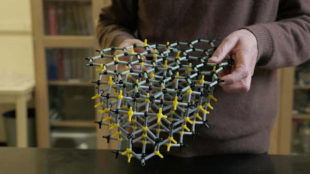
| Silicon and Graphene Models. |
 |
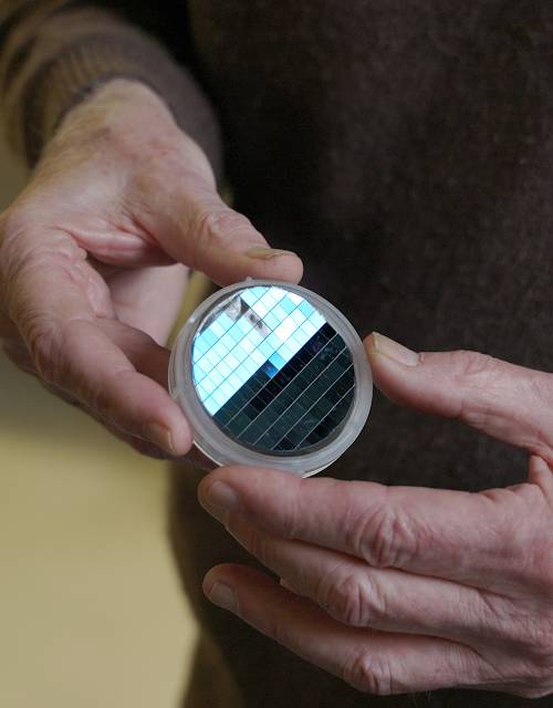
| Semiconductor Graphene Wafer |
The graphene revolution was originally driven by the search for electronic materials that could outperform silicon, Graphene, which is intrinsically a semi-metal (that is, a gapless semiconductor), was considered to be a probable candidate following predictions that, owing to quantum confinement, graphene nanoribbons can be semiconductors.
However, efforts to produce high-quality semiconducting ribbons were not successful". Therefore, research focused on altering the electronic structure of graphene chemically, but efforts failed to produce a viable semiconductor". After this, interest shifted away from graphene, towards other two-dimensional (20) materials that are intrinsically semiconducting".
The Georgia Tech researchers show that well-annealed epigraphene on a specific silicon carbide crystal face is a 20 semiconductor with very high mobility.
As a material, Epigraphene allows the quantum mechanical wave properties of electrons to be utilized, which is a requirement for quantum computing.
De Heer says that it will take time to develop this technology. “I compare this work to the Wright brothers’ first 100-meter flight. It will mainly depend on how much work is done to develop it.”


 IndianWeb2.com is an independent digital media platform for business, entrepreneurship, science, technology, startups, gadgets and climate change news & reviews.


